Holy Instrument · Suzhou Holy Instrument · Holy InstrumentOptical Inspection Instruments · QA Inspection Instruments · Metallographic Equipment
Hotline0512-65657743中文EnglishMobile13914063216Emailsuzhou@holyinst.com
Hotline0512-65657743
TECHNOLOGY & APPLICATION

PCB Evolution in the AI Server Era

Home/TECHNOLOGY & APPLICATION/PCB Evolution in the AI Server Era
PCB Evolution in the AI Server Era

AI servers are pushing PCB toward "semiconductor-grade" manufacturing

Over the past decade or so, server motherboards have typically had layer counts in the teens to twenties; on AI computing platforms, however, the layer counts of GPU compute boards, switch boards, and backplanes have undergone a non-linear leap. Based on public information, mainstream AI compute boards have evolved from 16-18 layer HDI to 20-22 layers and even 26 layer HDI, switch trays have reached over 30 layers, and orthogonal backplanes/midplanes have entered the range of 40-100 layers. An increase in layer count means copper-clad laminate and prepreg consumption multiply, the number of drilled holes rises by 20%-30%, and lamination alignment accuracy tightens to within 25 μm.
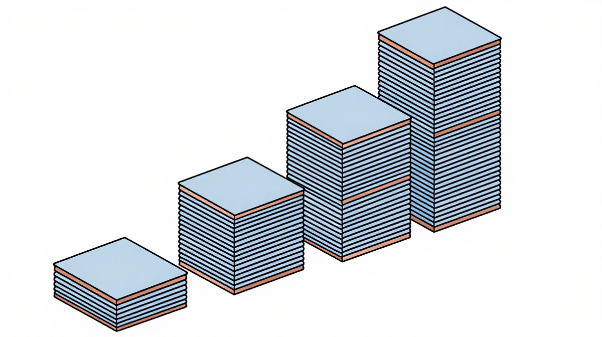
Schematic of PCB layer-count evolution for AI servers
Figure 3 — Schematic of PCB layer-count evolution for AI servers: from the teens to the 40-100 layer range (Schematic; a trend, not measured data)

Generational material upgrades: from M4 to M8/M9

  • Copper foil: to reduce high-frequency loss, surface roughness continues to decrease, ultra-low-profile copper foil (HVLP) has become mainstream, and new-generation platforms are beginning to adopt HVLP4/HVLP5
  • Fiberglass cloth: shifting from ordinary E-glass to Low-Dk/Low-Df systems, with quartz cloth (Q cloth) used in higher-end applications, significantly reducing dielectric constant and loss
  • Resin: iterating from epoxy systems to low-loss systems such as hydrocarbon resins and PTFE, supporting 112G/224G PAM4 signals in combination with M8/M9 grade copper-clad laminates

Process route: from subtractive to mSAP

800G and above optical modules and high-end HDI require further line width reduction. The traditional subtractive process has a physical limit due to the undercut effect, and the industry is gradually shifting to mSAP (modified semi-additive process). mSAP increases material utilization from about 50%-60% to around 90%, but process complexity rises significantly, and the value per board increases accordingly - which also means that process data collection and traceability requirements rise in tandem.
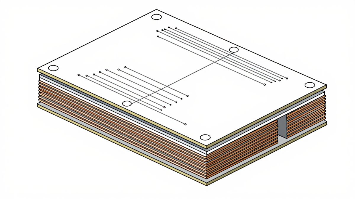
Schematic stackup cross-section of high-layer-count HDI and orthogonal backplane
Figure 4 — Schematic stackup cross-section of high-layer-count HDI / orthogonal backplane: interlayer copper, stacked vias and microvias (Schematic)

New requirements for inspection and measurement

  • Smaller hole diameters and higher aspect ratios: uniformity of copper thickness on hole walls is harder to guarantee, and the frequency and quantity of metallographic cross-section verification must both increase
  • Harder materials: high-hardness boards accelerate drill bit wear, causing greater variation in drilling quality, requiring cross-section data to reverse-correct drilling parameters
  • Thinner coatings and more complex structures: ENIG/ENEPIG gold layers are only 0.05-0.20 μm, requiring high-resolution XRF and cross-section data to corroborate each other
  • More layers: determination of defects such as inner-layer alignment, interlayer offset, and resin plugging relies more on cross-sections and 3D morphology observation

Our recommendations

As PCB process windows continue to narrow, "see it, measure it accurately, store it" becomes an absolute necessity: use metallographic cross-sections and digital/laser confocal microscopes to clearly confirm defects, use XRF and inline thickness measurement to quantify thickness data, and then let measurement data automatically enter the system for automatic judgment and archiving. Holy Instrument's metallographic specimen preparation equipment, digital microscopes, 3D measurement laser microscopes, and in-house measurement/SPC software are configured precisely around this chain.