
Hotline0512-65657743
Why Hole Wall Copper Thickness Is the Primary Reliability Indicator
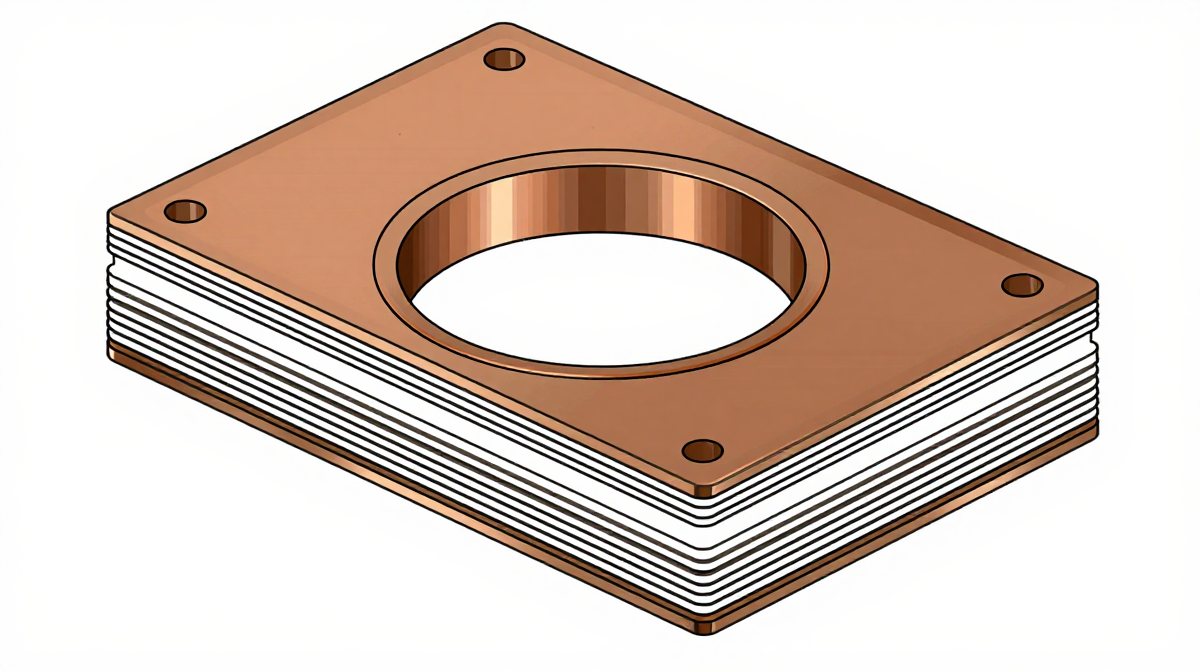
The copper layer on the walls of plated through holes (PTH) provides the main electrical and mechanical connection between layers. During assembly and service, the board undergoes multiple thermal cycles, and locations with thin hole copper become stress concentration points: microcracks appear first, then gradually propagate into an open circuit. This is precisely why IPC-6012 specifies a minimum average hole wall copper thickness - Class 2 (general commercial and consumer products) requires an average hole wall copper thickness of approximately 20 μm, while Class 3 (high-reliability applications such as medical, automotive, and aerospace) requires approximately 25 μm, with stricter defect limits on hole wall voids, cracks, and plating separation.
Aspect Ratio Determines Process Difficulty
The deeper the hole and the smaller the diameter, the harder it is for chemicals and current to penetrate uniformly into the hole, and the copper layer at the center of the hole is often the thinnest (commonly known as the "dog bone" effect). The industry generally regards 8:1 as the comfort zone for conventional processes, while ratios above 10:1 typically require pulse plating combined with more precise additive control. As high-layer-count boards reduce hole diameters to the 0.15 mm range and board thickness continues to increase, the difficulty of aspect ratio control rises accordingly. Copper thickness data for such products must be verified batch by batch using microsections, rather than relying solely on non-destructive sampling inspection.
Several Key Parameters for Copper Thickness Control
Surface Treatments Have Their Own Thickness Standards
Electroless nickel immersion gold (ENIG) per the IPC-4552 series requires a gold layer of 0.05-0.20 μm and a nickel layer of approximately 3-5 μm; immersion silver approximately 0.1-0.3 μm, immersion tin approximately 0.8-1.2 μm, and OSP approximately 0.2-0.5 μm. Insufficient coating thickness affects solderability and storage life, while excessive thickness may cause issues such as gold embrittlement and reduced solder joint strength. Therefore, "thickness" must be quantitatively measured rather than judged by experience.
Applicable Boundaries of Various Thickness Measurement Methods
Recommended Closed-Loop Control System
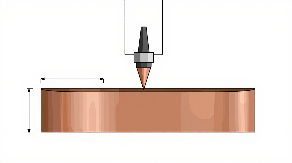
Link three sets of data - plating chemical analysis (e.g., monitoring additive concentration using the CVS cyclic voltammetric stripping method), in-line copper thickness monitoring, and metallographic cross-sections before shipment - to form a closed loop of "chemistry-current-thickness-judgment," so that the process capability index (Cpk) becomes truly meaningful. Holy Instrument can provide a complete supporting solution covering metallographic cross-section specimen preparation (precision cutting, mounting, grinding and polishing), metallographic/digital microscope observation, XRF coating thickness measurement, in-line copper thickness measurement, and SPC data analysis.