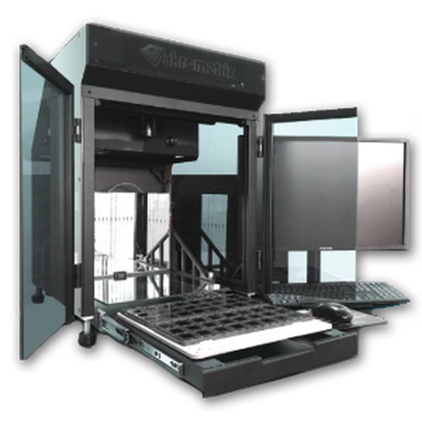
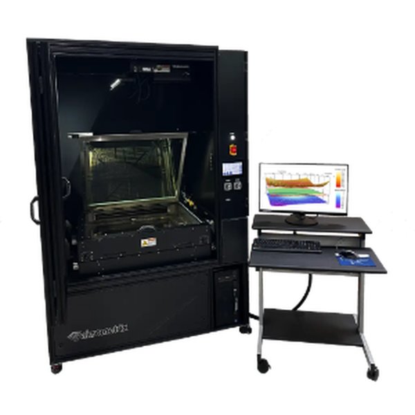
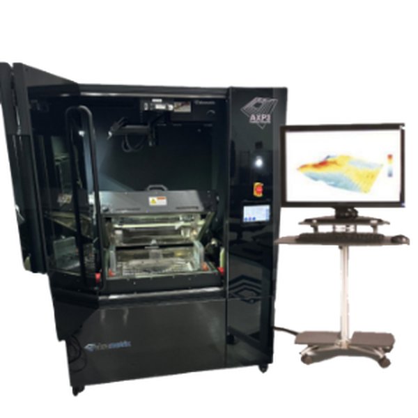
Akrometrix Thermal Warpage & Strain Measurement System uses Shadow Moiré technology for warpage, coplanarity and strain measurement of PCB, substrates, ICs, packages, wafers and panels under various temperature profiles.
Core Capabilities
- Warpage measurement over temperature profiles: -50°C to 300°C
- Applicable to: chips, components, PCB, stacked chips, wafers, wafers on film frames, panels
- z-axis resolution down to 0.85 μm
- Full-field image data acquisition in less than 2 seconds
- Sample size range: 2 mm x 2 mm to 610 mm x 600 mm
Software Functions
- Predicts the fit of two substrates / chips / PCBs over a temperature profile, particularly suitable for measuring the warpage effects of different material layers laminated together
- Measurement matrix generator: divides a large area into multiple sub-areas for simultaneous global and local warpage measurement
- Sample tracking: multiple samples can be loaded into the heating process simultaneously; the software automatically distinguishes each sample, performs rotation compensation and reports warpage data separately
- Die tilt analysis: measures the relative angle between the die and the substrate surface for reflow or die attach interface analysis
Models & Specifications
| Model | Technology | Max. Substrate Size | z Resolution | Temperature Range |
|---|
| AXP 2.0 | Shadow Moiré thermal warpage measurement | 375 x 400 mm | 0.85 μm | -50°C ~ 300°C |
| PS200S | Shadow Moiré thermal warpage measurement | 200 x 200 mm | 0.85 μm | 25°C ~ 300°C |
| PS600S | Shadow Moiré thermal warpage measurement | 610 x 600 mm | 1.5 μm | 25°C ~ 300°C |
| AKM600P | Dedicated to thermal warpage measurement of FOWLP panels / wafers | 610 x 600 mm | 1.5 μm | 25°C ~ 300°C |
| TT-SM | Benchtop, room-temperature Shadow Moiré warpage measurement only | 325 x 300 mm | 0.85 μm | Room temperature |
Optional Modules
- DFP (Digital Fringe Projection): can be added to AXP 2.0, PS600S or AKM600P for measuring discontinuous surfaces with large step changes in surface height
- DIC (Digital Image Correlation): can be added to AXP 2.0 or PS200S for substrate thermal strain (x, y) measurement down to 150 microstrain
- CRE (Convection Reflow Emulator): can be added to AXP 2.0 to simulate the uniformity and heating rate of a reflow oven
Testing Services: Flatness, warpage and coplanarity measurement of PCB / substrates / ICs / packages / full wafers and wafers on film frames; in-plane deformation (strain) and CTE measurement; sizes from 2x2 mm to 600x600 mm; dynamic temperature profiles from -50°C to 300°C. Testing is performed at the application laboratory in Atlanta, USA, with a turnaround time of 2-10 days.